Research on Nano-artifact Metrics (NAM)
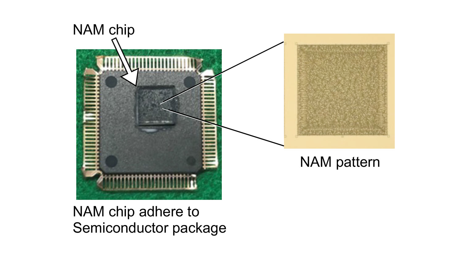
The distribution of counterfeit products or parts with high added value causes disruption to the supply chain, such as disadvantages for legitimate vendors and users. If you can create a unique tag which is physically difficult to create the same thing, you can prevent or detect the distribution of counterfeit products by attaching it to the product you want to protect. As a candidate for such tags, we are developing nano-artifact metrics (NAM) technology that forms random nanoscale patterns using processes caused by fluctuation in the semiconductor manufacturing process. The prototype is made of a very stable material such as silicon or quartz, and its chip shape makes it easy to mount on various products and parts.
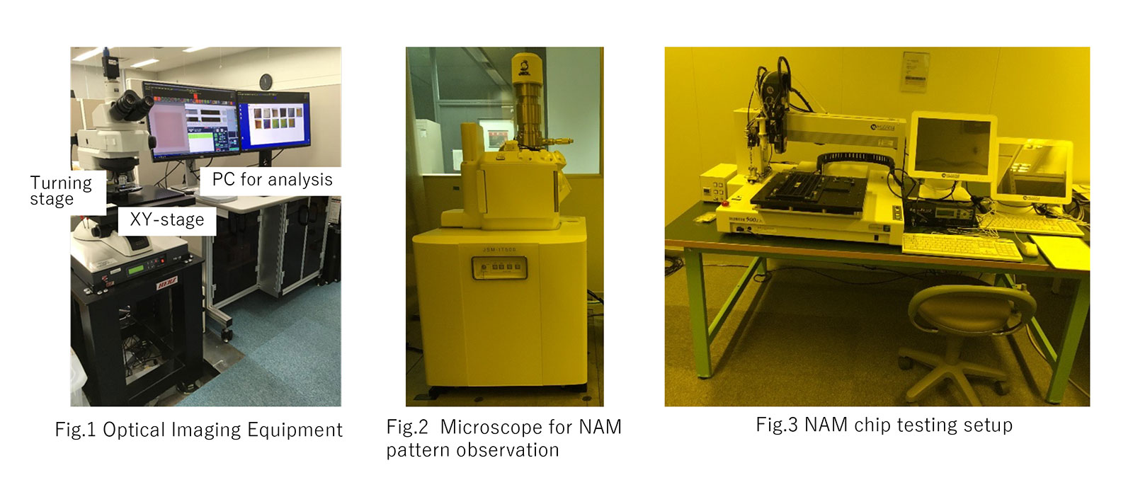
We have prepared an analysis environment to evaluate the prototype NAM pattern. The photo shows a device that acquires optical images (Fig. 1), a device that observes nanoscale NAM patterns (Fig. 2), and a device that mounts and prototypes a large number of NAM chips (Fig. 3).
Reference
- T. Matsumoto, M. Hoga, Y. Ohyagi, M. Ishikawa, N. Naruse, K. Hanaki, R. Suzuki, D. Sekiguchi, N. Tate, M. Ohtsu, “Nano-artifact metrics based on random collapse of resist”, Sci. Rep. 4, 6142 (2014)
- T. Matsumoto, N. Yoshida, S. Nishio, M. Hoga, Y. Ohyagi, N. Tate, and M. Naruse, “Optical nano artifact metrics using silicon random nanostructures”, Sci. Rep. 6, 32438 (2016)
- Hiro Nodaka, Ami Tezuka, Hiroyuki Kuwae, Kosuke Yamada, Morihisa Hoga, Haruo Shimamoto, Shuichi Shoji, and Jun Mizuno、“QFP/quartz adhesive bonding with surface treatment for physical security of edge artificial intelligence devices”, Transactions of The Japan Institute of Electronics Packaging, Vol.13, E20-008-1-E20-008-4 (2020)